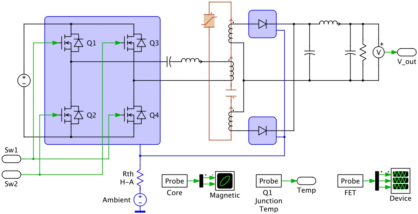
Below is a PLECS demo model of an isolated DC/DC resonant converter operated under frequency control. The output voltage of the converter is controlled by changing the switching frequency of the semiconductors. Zero-Voltage Switching (ZVS) is used to reduce switching losses, allowing the operation of the converter at higher switching frequencies.

Power circuit
The LLC converter is a DC/DC converter with a front end H-bridge. The AC side of the H-bridge is connected to the primary side of a high frequency transformer via a series-connected resonant inductor and capacitor. The magnetizing inductance of the transformer, along with the inductor and capacitor, form the LLC resonant tank. The secondary side of the transformer is connected to a full wave diode rectifier to convert the AC transformer output to a high ripple DC voltage that is then filtered to provide a low ripple DC voltage output.
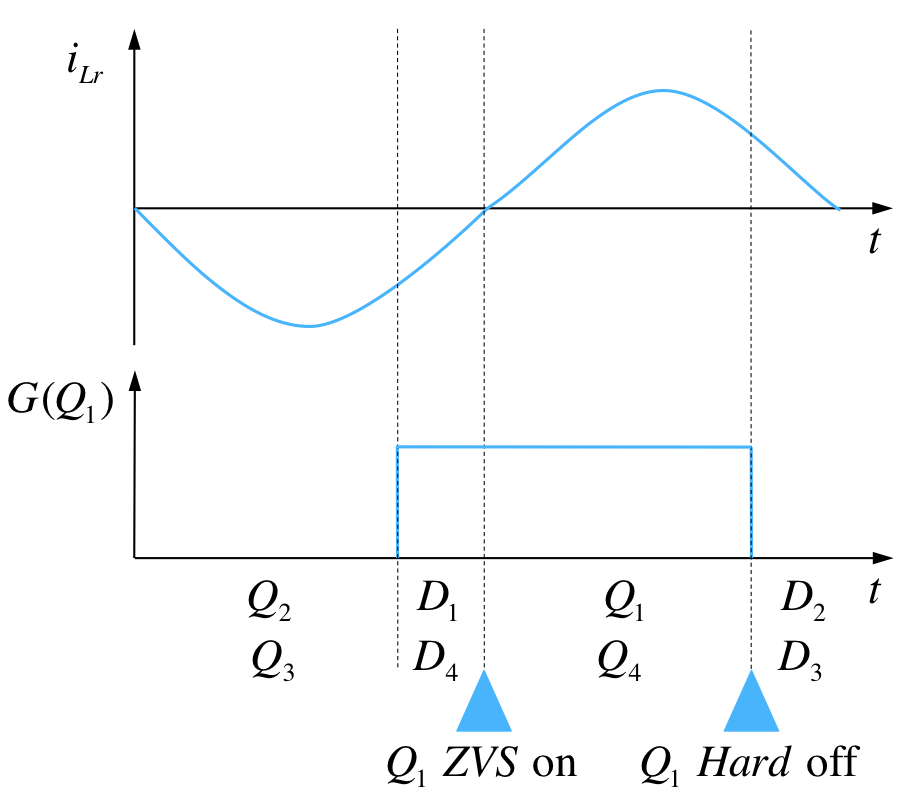
The LLC converter is often operated under zero-voltage switching (ZVS) operation where each FET (e.g., Q1) is turned on when the current is still flowing in its respective anti-parallel diode (e.g., D1). Therefore, only the forward voltage drop of the diode is applied to the FET, which is small compared to the DC input voltage. This results in negligible turn-on loss in the device and contributes to the reduction of overall losses. During ZVS operation, the FETs are turned off in a region where they conduct current. This results in hard-switching of the devices, generating turn-off switching losses, as shown below.

During turn-off and turn-on events, the body capacitor of each FET is charged and discharged, respectively. For circuits where the FETs (not the reverse diodes) experience hard-switching during turn-on, the charge stored in the body capacitor is dissipated through the FET, adding to the switching losses. These losses can be captured in simulation (without adding a capacitor parallel to the FET) by simply including them in the thermal loss look-up tables for a specific part. When measuring the switching energy losses of FETs for certain operation points to generate the loss look-up table, it is important to include the charge stored in the FET body capacitor in the loss measurements. A major advantage of ZVS for FETs, in addition to eliminating turn-on losses, is that the energy stored in the body capacitance is recycled into the circuit, assuming there is enough blanking time between turn-off of Q1/Q4 and turn-on of Q2/Q3. Therefore, in soft-switching topologies operated with ZVS, turn-off losses can be overestimated by 10 to 20%, if the effects of the capacitive elements are not reflected in the loss look-up tables.
Control
The output voltage is measured by a sensing circuit, simplified here as a transfer function (representing a low pass filter). A simplified ADC module is use to convert the measured voltage into its corresponding digital value. The output voltage measurement is compared against a DC voltage setpoint. The error is fed into a 2-pole, 2-zero implementation of a digital PI controller. An ADC interrupt is used to trigger the interrupt service routine to run the controls (simulated here as a triggered subsystem). The controls generate a counter period setpoint that is then converted into a frequency setpoint. The frequency setpoint is used by the PLECS variable frequency carrier. The half-bridge FETs are switched with a 50% duty cycle. The LLC variable frequency controls can also be implemented using high fidelity ADC and PWM peripheral models that are available in the PLECS Processor-in-the-Loop (PIL) component library.
Simulation
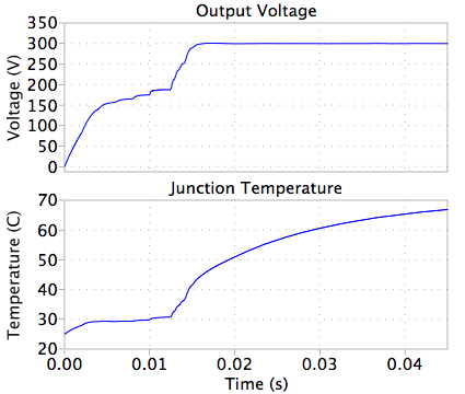
A 200 VDC input is connected to the DC side of the full bridge. A slew rate is applied to the converter to limit the rate of change in output voltage during changes in reference voltage. Additionally, a soft start algorithm is employed to limit the rate of change in commanded voltage during startup. This is reflected on the startup transient as the output voltage incrementally ramps up. After the soft start, a voltage controller is used to control the full bridge switching frequency. The system reaches the desired 300 VDC output after 20 ms. The plot below shows the transient simulation of the LLC converter from startup.

PLECS thermal descriptions are provided for the semiconductor devices. The body capacitor’s energy storage is not included in the lookup table for this model; therefore the turn-off loss yields a maximum 20% overestimate, as previously discussed. The soft switching strategy maintains FET junction temperatures at a safe temperature range while switching at high frequency. Additionally, engineers can size magnetic components using the PLECS Saturable Core block to operate the system at the desired point of the B-H curve, which can be observed using the PLECS XY Plot component.
Try it
This model is available in the PLECS Demo Model library provided in both versions of PLECS.
